itutorial - N channel MOSFET or often referred to as NMOS when using enhancement mode has the characteristic of normally off or does not conduct when there is no voltage at the Gate-Source (V GS ) terminal , so the NMOS will conduct only if there is a positive voltage at the Gate-Source where the voltage is V GS must be greater than the threshold voltage ( VTH ). V TH is the minimum voltage at the Gate-Source terminal so that the MOSFET can flow electric current to the Drain-Source terminal .
Characteristics of N-channel MOSFET enhancement mode
The characteristics of the NMOS enhancement mode shown in Figure 1 depict the transconductance slope plot when the voltage V DS remains constant or does not change with V GS changing from 0 to positive.
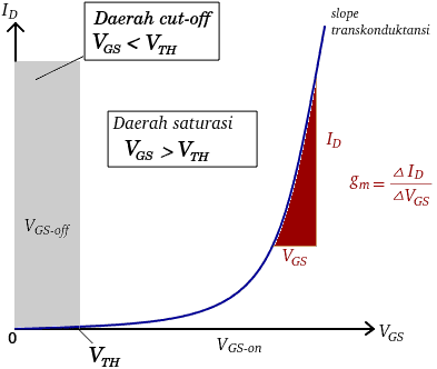 |
| Figure 1. Characteristics of N-MOSFET enhancement mode |
The amount of Drain current (I D ) in the N-MOSFET enhancement can be calculated using the formula:

k : The magnitude of the conductance parameter.
V GS Q : The amount of dc voltage at the Gate-Source .
V TH : The magnitude of the threshold voltage at the Gate-Source .
V DS : Voltage at the Drain-Source terminal .

DC Bias N-Channel E-MOSFET
 |
| Figure 2. E-MOSFET working point |
Basic Common Source Amplifier Using N-Channel E-MOSFET
Figure 3 shows the basic amplifier circuit using a Common Source E-MOSFET with the following explanation:
- C 1 : Used to block dc current from flowing to the signal source. Apart from that, C 1 also functions as a coupling where the ac current will be superimposed on the dc current from the V DD source . C 1 also functions as a high pass filter which will pass signals with a certain minimum frequency.
- C 2 : Used to block dc current from V DD so that only ac current comes out of the capacitor. C 2 together with R D and R Load forms a high pass filter which transmits signals with a certain minimum frequency.
- R 1 and R 2 are resistors to provide voltage to the Gate terminal so that the E-MOSFET can work. The magnitude of the voltage at the Gate terminal depends on the value of R 1 and R 2 with V G = [R 2 / (R 1 + R 2 )]. V DD
- Resistor R D is used to limit the current flowing at the Drain and load terminals ( R Load )
- R S : Used to get the voltage at the Source terminal so that the desired V G S is obtained .
- VDD= 12 Volts,
- VTH = 2 Volts
- k = 0.0006 A/V2
- RD= 3.3kΩ
- R
- λ = 0.01/Volt
- Ignoring Gate width (W) and Gate length(L) .
 |
| Figure 3. Basic N-MOSFET amplifier mode enhancement |
DC Analysis
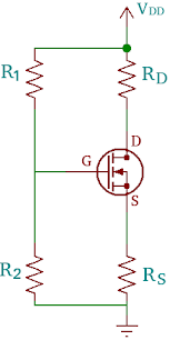 |
| Figure 4. DC analysis of N-MOSFET |
Calculate all required component values in Figure 4 with the data provided above:
Answer:
V D = 6 Volts.
I D Q = V D / R D
I D Q = 6 Volts / 3300Ω
Second step: Find the voltage V GS that causes the N-MOSFET to conduct. In dc analysis the value of λ can be ignored because the value is very small.
V GS = √(I D /k) + V TH
V GS Q = 3.741 Volts
 |
| Figure 5. Components of dc analysis calculations |
The working point ( Q ) of dc bias is shown in Figure 6.
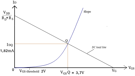 |
| Figure 6. Working point (Q) graph of dc N-MOSFET |
Determine the values of C 1 and C 2
 |
| Figure 7. Common source N-MOSFET amplifier circuit |
AC analysis


g m : Transconductance.
V GS : Voltage at Gate Source ac analysis.
I D : Current at the ac analysis Drain terminal .
In ac analysis, each capacitor will be considered short connected between its terminals. For the amplifier circuit in Figure 3, it is necessary to create an equivalent ac analysis circuit shown in Figure 8.
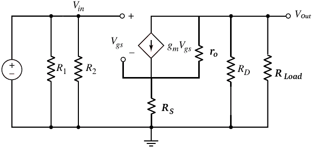 |
| Figure 8. Common source analysis equivalent circuit |
From the AC analysis equivalent circuit image above, it is used to calculate the amount of MOSFET gain .


V out = g m . V GS . Z out
g m = 2 . k. (V GS – V TH )
g m = 2 . 0.0006 . (3.741 Volts – 2 Volts)
g m = 0.0021 A/V
g m = 2.1 mA/V
A V = (g m . Z o ut ) / (1 + g m . R S )
A V = (2.1mA/V . 2481 Ω ) / (1 + 2.1mA/V . 142 Ω )
A V = (2.1mA/V . 2481 Ω ) / (1 + 2.1mA/V . 142 Ω )
A V = (5.2) / (1.29)
A V = 4
Common Source Amplifier uses a capacitor at the Source terminal ( bypass capacitor ) .
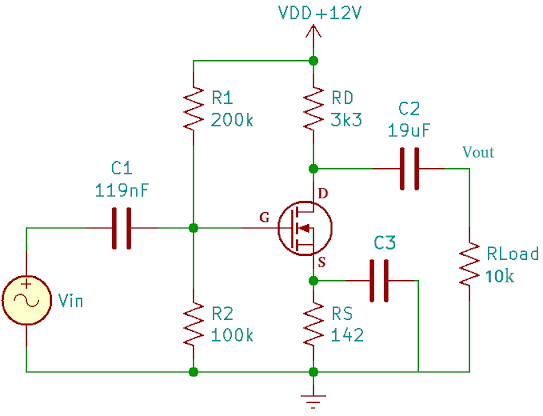 |
| Figure 9. Common source amplifier using capacitor bypass |
To determine the working point ( Q ) of the MOSFET is exactly the same as the dc analysis above. Meanwhile, for ac analysis to calculate the amount of gain for the amplifier circuit, it is shown in Figure 10.
 |
| Figure 10. Equivalent AC analysis circuit with a capacitor at the source terminal |
The ac analysis equivalent circuit of Figure 10 does not have R S even though it actually has R S in the amplifier circuit. This is because in the AC equivalent circuit analysis each capacitor is considered short connected . For small signals , r o is considered to be so large that it can be ignored.
From Figure 10 and r o is ignored, the magnitude of the gain of the common source amplifier circuit using a capacitor at the source terminal is as follows:
V out = g m V GS . Z out
V in = V GS -> K because capacitor C 3 is considered short-circuited.
So:
A V = V out / V in
A V = g m V GS . Z out / V GS
A V = g m . Z out
A V = 5.2
From the ac analysis gain calculation it can be concluded that using a bypass in the common source can increase the signal gain.To determine the magnitude ofC 3 , it must be determined at what frequency the capacitor will work to help increase the gain. Because the amplifier circuit is intended to strengthen sound signals, when the frequency is 20Hz the capacitor can work to help increase the gain so thatC 3 can be found as follows: C 3 = 1 / (2 . π . f . R S ) C 3 = 1 / (2 . π . 20Hz . 142 Ω ) C 3 = 1 / (2 . π . 20Hz . 142 Ω ) C 3 = 56 µ F
'Eelektronika' 카테고리의 다른 글
| Rectifier diode (0) | 2024.04.26 |
|---|---|
| PWM Arduino Uno (0) | 2024.04.26 |
| JFET (Junction Field Effect Transistor) (0) | 2024.04.26 |
| Scissors & Tongs (0) | 2024.04.26 |
| Install Sloeber IDE on Windows (0) | 2024.04.26 |